
ASML High-NA EUV: The Machine Behind Strategic Chip Power
The ASML TWINSCAN EXE platform is more than just a semiconductor printer. This is a strategic manufacturing capability that leverages plasma physics, atom-scale metrology, ultrahigh vacuum engineering, and precision motion control. High Numerical Aperture Extreme Ultraviolet (High-NA EUV) lithography is of growing importance to sophisticated computing, artificial intelligence and the semiconductor supply chains underpinning modern military systems and was developed in the Netherlands through an international industrial network.
However, its importance must be precisely defined. The machine patterns individual layers of integrated circuits onto silicon wafers. It does not produce complete chips. Neither its 8-nanometre optical resolution nor its 2-nanometre technology-node designation is a literal transistor-gate length.
Optical Resolution: Why 0.55 NA Matters
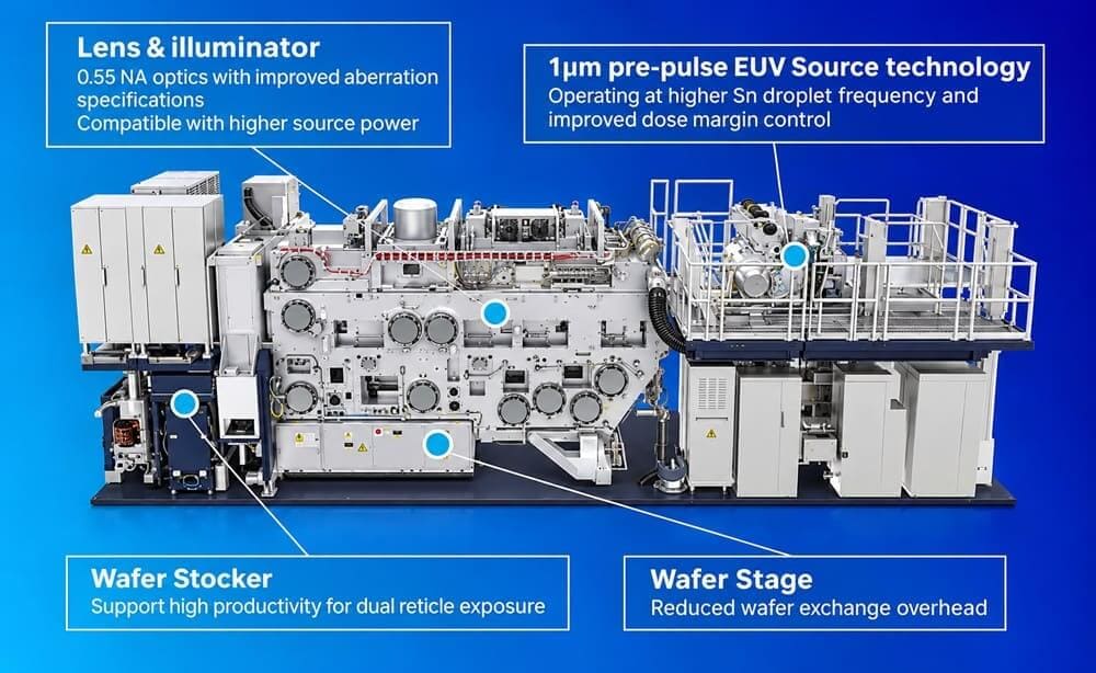
Traditional EUV scanners have a numerical aperture (NA) of 0.33 and a wavelength of 13.5 nm. In the EXE:5000, ASML raised the NA to 0.55, which increased the nominal single-exposure optical resolution from approximately 13 to 8 nanometres. The Rayleigh relation shows this improvement:
CD = k 1 λ / NA
CD is the minimum printable critical dimension, λ is the exposure wavelength, NA is the numerical aperture and k1 is the process-dependent imaging factor. At constant wavelength and k1, higher NA results in smaller features. ASML estimates that the resulting 1.7x reduction in minimum printable feature size enables as much as 2.9x higher two-dimensional feature density for comparable patterning conditions.
This represents theoretical lithographic scaling potential, not a threefold increase in finished-chip transistor counts. EXE also delivers about 40% better imaging contrast than conventional NXE technology, potentially easing some patterning defects and exposure-dose requirements. Another complication of high NA is that the depth of focus is typically inversely proportional to the square of the numerical aperture. Engineers therefore need better control over wafer topography, resist thickness, thermal deformation, and optical aberrations.
Tin Plasma Generates Extreme Ultraviolet Light
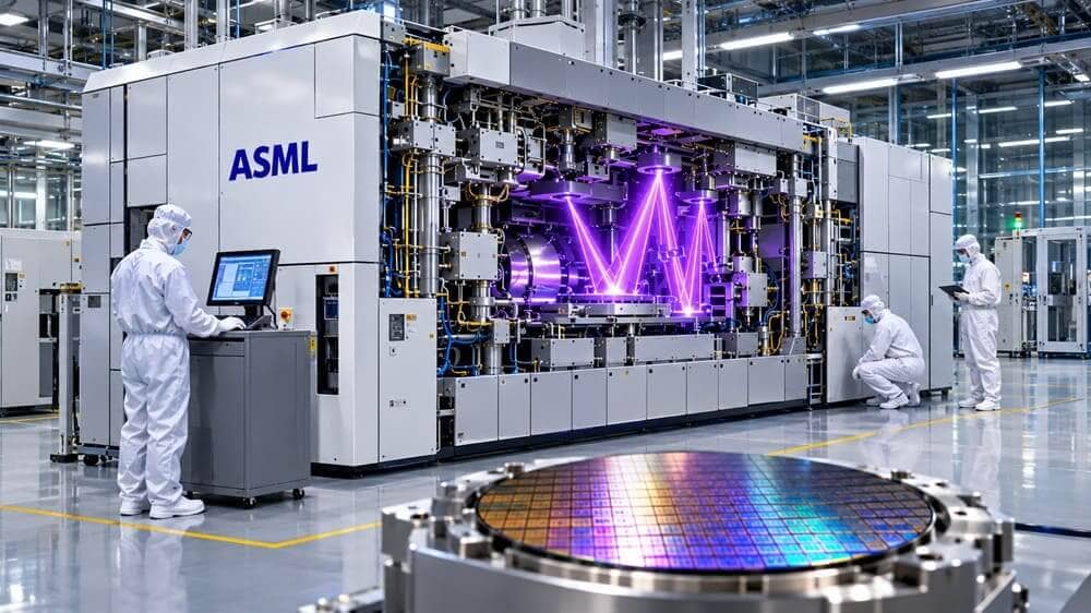
Normal atmospheric optical paths and conventional refractive glass optics are not efficient for propagation of EUV radiation. Hence, the scanner employs vacuum optical paths and multilayer reflective mirrors. ASML’s laser-produced plasma source fires molten tin droplets of about 25 micrometres in diameter at about 70 metres per second. A preparatory laser pulse flattens each tin droplet before a more powerful pulse vaporises it into EUV-emitting plasma. In ASML’s documented source design, this interaction happens some 50,000 times a second.
The resulting plasma can be heated to temperatures as high as 220,000 °C, about 40 times hotter than the Sun’s photosphere. The phenomenon is, however, fundamentally different from normal sustained heating due to its microscopic dimensions and extremely short lifetime. To obtain enough usable EUV power, droplet generation, laser targeting, plasma formation and optical collection have to be very well synchronised. Tin debris, contamination and mirror degradation also plague source engineers. Even small losses in reflectivity can reduce available illumination and manufacturing throughput.
ZEISS Mirrors: Atomic Precision
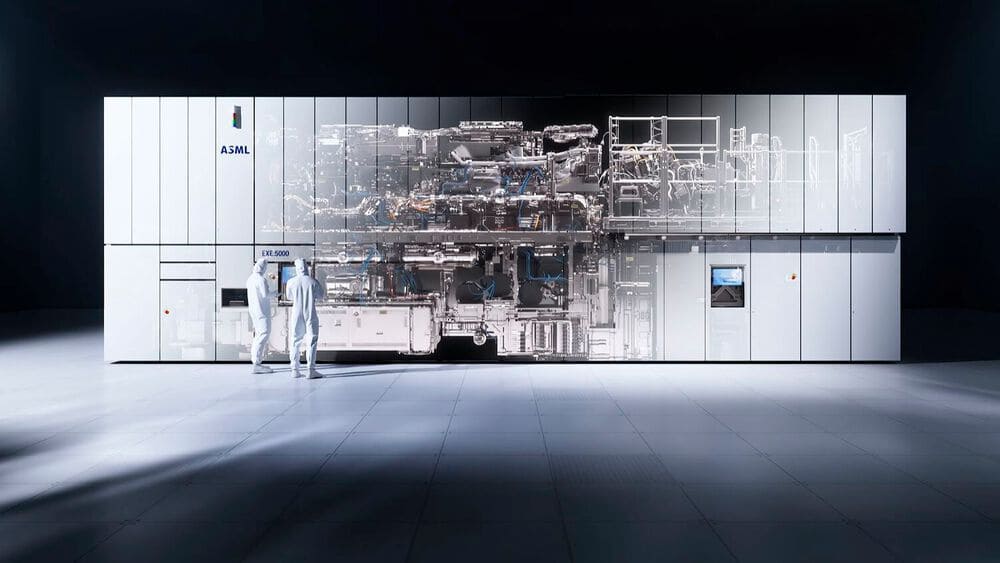
ZEISS Semiconductor Manufacturing Technology in Germany makes speciality optical assemblies for EUV lithography. The High-NA projection optics assembly consists of over 40,000 individual parts and has a weight of approximately 12 metric tonnes. The separate illumination system weighs some 6 metric tonnes. ZEISS manufactures multi-layer mirrors with more than 100 layers. Some take a year to make. Furthermore, the company has created special measuring systems that can measure extremely small deviations in surfaces. A key engineering innovation is anamorphic demagnification. The high-NA optics reduce the photomask pattern by a factor of four in one direction and by a factor of eight in the other, rather than reducing it uniformly in both directions.
This configuration accommodates the optical geometry required for High-NA EUV while retaining conventional reticle dimensions. However, it also shrinks the exposure field by about 1/2 of the conventional EUV systems. Therefore, large semiconductor layout generation may need field stitching, extra exposures and tighter alignment steps. To solve the productivity problem, ASML has built stages that can accelerate very fast. The published EXE architecture has wafer stage acceleration of approximately 8g and reticle stage acceleration of up to 32g. Engineers must maintain nanometre-scale positioning and overlay accuracy despite these extreme accelerations.
Case Study: Intel’s Industrial High-NA Breakthrough
In April 2024, Intel completed the installation of the first commercial ASML EXE:5000 at its Hillsboro, Oregon development facility. According to Intel, the assembled High-NA EUV system weighed approximately 165 tonnes. The transport and installation showcased the logistical challenge of getting advanced lithography systems into semiconductor fabrication facilities. September 7, 2026 – Intel Foundry and ASML announce that more than 1 million wafers have been processed on High-NA EUV equipment. Notably, this total included equipment certification, testing, research, development, and commercial manufacturing exposures on selected layers of some Intel Core Ultra Series 3 processors, code-named Panther Lake.
The one-million-wafer milestone included equipment certification, research, development, and high-volume manufacturing, rather than representing one million finished, commercially saleable wafers. Intel also said that in selected cases, High NA patterned Intel 18A layers matched or exceeded the performance of comparable layers produced using conventional 0.33-NA EUV. The milestone showed practical industrial integration, but the announcement did not reveal full manufacturing yields, customer-specific defect densities, or confidential per-chip production costs.
Military Applications and Significance
The newest techniques in lithography are allowing for the development of processors that contain more computing power and consume less energy. These capabilities could be used to power artificial-intelligence accelerators, electronic-warfare processing, intelligence analysis, satellite-image exploitation and advanced military command and control architectures. Meanwhile, not every military electronic system needs the most advanced semiconductor nodes. The more mature fabrication technologies are deliberately chosen for many radar, aerospace and radiation-hardened applications, as reliability, qualification and operational durability are more important than transistor density.
A major strategic vulnerability in advanced lithography arises from the concentration of specialised manufacturing capabilities within a limited international supplier network. ASML depends on specialised companies in different countries for precision optics, laser technology, mechatronics, advanced materials and supporting manufacturing systems. Replicating an advanced lithography scanner alone would not reproduce the materials, software, metrology, and process-integration infrastructure required for high-volume semiconductor manufacturing.
Countries also require photoresists, photomasks, inspection equipment, computational lithography, process integration expertise and stable industrial supply chains. That concentration of technology has also turned semiconductor manufacturing equipment into a national security issue. On December 2, 2024, the US Bureau of Industry and Security announced new controls covering 24 types of semiconductor manufacturing equipment and three types of related software, primarily targeting China’s advanced semiconductor manufacturing capabilities and associated military applications. These controls illustrate the strategic value of advanced semiconductor manufacturing, not that military weapons factories are using High-NA EUV equipment.

Proprietary Engineering and Capabilities
Critical engineering parameters and production data remain proprietary. Such details include customer-specific process recipes, aberration-correction parameters, contamination thresholds, stochastic defect distributions, equipment availability, field-stitching yields and long-term source-power stability. These are variables that determine how consistently profitable industrial manufacturing can be derived from laboratory-scale optical achievements. Without verified disclosures on these confidential parameters, any speculation would remain just that: mere speculation.
Conclusion
High-NA EUV lithography is a blend of advanced optical physics, plasma engineering, precision robotics, semiconductor chemistry, and international industrial collaboration. The process is more than just making smaller transistors. Its strategic importance lies in enabling advanced semiconductor manufacturing and strengthening the industrial foundations of modern computing and national security.
The main advantage is not the machine, but the industrial system that can build, service and upgrade it continually. In the strategic race for semiconductor supremacy, technological sovereignty ultimately depends on robust manufacturing ecosystems, top-tier engineering talent and dependable access to essential equipment.
References
- ASML. 5 Things You Should Know About High-NA EUV Lithography. January 25, 2024.
https://www.asml.com/en/company/stories/2024/5-things-high-na-euv - ASML. Light and Lasers: Creating EUV Light. Technical documentation.
https://www.asml.com/en/technology/lithography-principles/light-and-lasers - ZEISS Semiconductor Manufacturing Technology. High-NA EUV Lithography: The Next EUV Generation.
https://www.zeiss.com/semiconductor-manufacturing-technology/inspiring-technology/high-na-euv-lithography.html - Intel Foundry. Intel and ASML Collaborate to Accelerate Industry Readiness for High NA EUV. September 7, 2026.
https://www.intel.com/content/www/us/en/newsroom/news/intel-foundry/intel-foundry-asml-accelerate-industry-readiness-for-high-na-euv.html
About the Author